There are a number of devices based on semiconducting junctions which serve niche purposes in the industry. The most prominent example is the Bipolar Junction Transistor (BJT). More specialized devices include the Heterojunction Bipolar Transistor (HBT) and the Junction Field Effect Transistor (JFET).
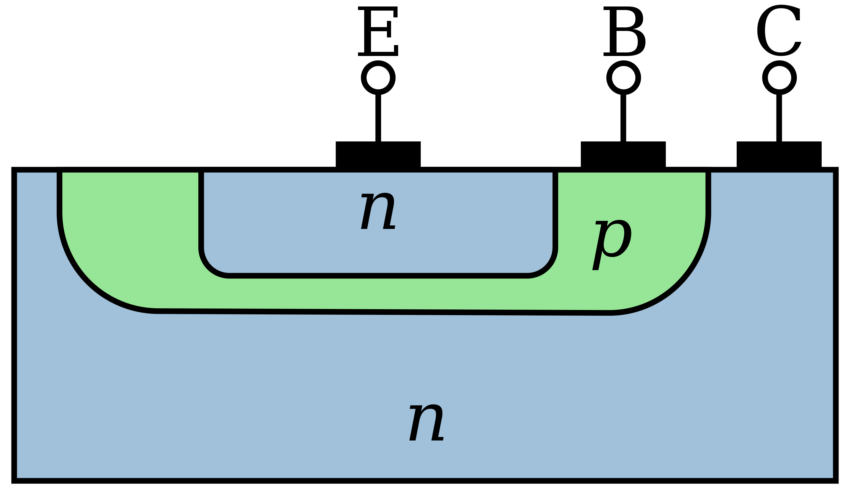
A typical BJT device cross-section is shown in the figure below. The key aspects of its design are its very thin Base region and a strong Emitter doping compared to the Base doping. At the Base-Emitter junction, the depletion region extends into the Base. When this junction is forward-biased, while the Base-Collector junction in reverse biased, minority carriers are generated at the edge of the depletion region within the base, very close to the Collector junction. The newly generated carriers are closer to the Collector region than the material’s diffusion length, which means most generated carriers diffuse across the junction before they recombine. The small Base current is mostly due to recombination.

In a typical BJT structure, like the one shown above, the Base and Emitter terminals are “nested” inside of the Collector. The Collector has weak doping with donors, then the Base is created by implanting a much stronger layer of acceptor dopants over top of the donors. The Emitter is again a much stronger layer of donors implanted over top of the Base. Due to this nesting configuration, BJT devices have not scaled to the nano regime like MOSFETs have.
Since the fraction of recombining carriers is mostly determined by the device’s geometry, the BJT has a nearly constant current gain \(\beta\). There are a few factors that can change \(\beta\):
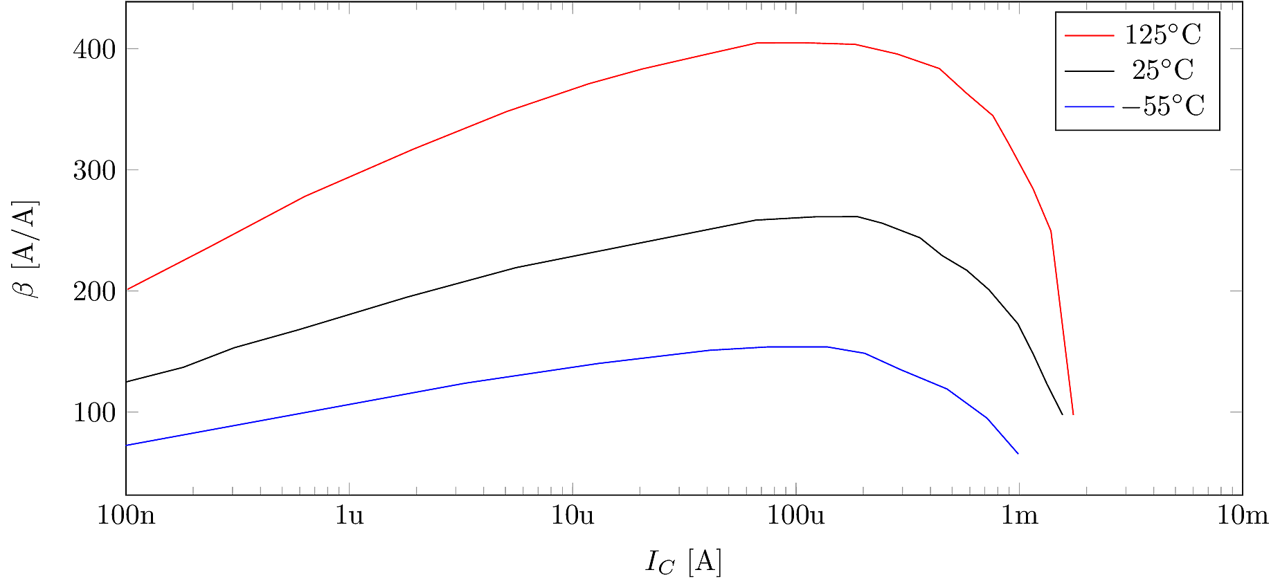
High-Level Injection: when the collector current is large, the mobile electron concentration will exceed the Base doping concentration. At this point the physics changes, and \(\beta\) drops precipitously.
Surface Leakage: when the collector current is small, it becomes comparable to Base-Emitter leakage currents which do not go through the junction, and do not get amplified. As a result, \(\beta\) declines.
Temperature: since the BJT’s operation depends on diffusion length, which is a property of random motion due to heat, we should expect \(\beta\) to chance with temperature. Intuitively, at higher temperatures there is more energy, so we expect a greater diffusion length and therefore a higher \(\beta\).
Frequency: the BJT is based on diffusion, which takes some time. The Base Transit Time \(\tau_F\) is the average time a charge carrier takes to exit the base. The device’s unity gain frequency (aka transit frequency) is \[f_T = \frac{1}{2\pi \tau_F}.\] At \(f_T\), \(\beta=1\). The device’s cutoff frequency is found by applying the gain-bandwidth product: \[f_C = \frac{f_T}{\beta_0},\] where \(\beta_0\) is the device’s gain at low frequencies.
BJT data sheets usually show curves indicating how \(\beta\) varies as a function of collector current, temperature and frequency (note: \(\beta\) is often reported using the symbol \(h_{FE}\)). Some example curves are shown in the figure below. In this example, the device has maximum \(\beta\) for \(I_C \sim 100\mu\)A. This peak location depends on the device’s materials, size, geometry, doping, etc. Some devices may have maximum \(\beta\) at 10mA or 100mA — it’s always prudent to study the datasheet and match the device to its application.

When the Emitter and Base are constructed from different semiconductor materials, they form a heterojunction. The different materials allow the energy bands to be manipulated so as to suppress the flow of carriers from the Base to the Emitter. In particular, the Emitter material should have a larger bandgap than the Base material. The theory was developed by Herbert Kroemer in a 1957 paper, and he was later awarded the Nobel Prize in 2000 (shared with Jack Kilby for inventing the integrated circuit). Kroemer’s abstract offers a good summary of the heterojunction concept:
In order to obtain a high current amplification factor, it is important in transistors that the ratio of the injected minority carrier current over the total emitter current, \(\gamma\), be close to unity, or that the quantity \(1-\gamma\), called the injection deficit, be as small as possible. It is shown that the injection deficit of an emitter can be decreased by several orders of magnitude if the emitter has a higher band gap than the base region. This effect can be utilized either in addition to the commonly used high emitter doping in order to eliminate the alpha falloff with current, or to decrease the high emitter doping in order to obtain a lower emitter capacitance. Decreasing the emitter capacitance in high-frequency transistors may be utilized either to extend their frequency range or to increase their power capabilities by increasing the area.
It was shown that if the bandgap difference is \(\Delta E_g\), then the device’s current gain (i.e. \(\beta\)) can be boosted by a factor of
\[\text{Gain Muliplier} = e^\frac{\Delta E_g}{kT}.\]
In addition, HBTs have reduced capacitance and much higher transit frequency than homojunction BJTs. In Radio Frequency (RF) HBTs, an ultra-thin Base region is used to minimize the transit time (hence maximizing the transit frequency). In a homojunction BJT, the Base thickness is limited by punch-through breakdown: if the Base is too thin, the Collector and Emitter depletion regions can merge, allowing a high current to pass which can ultimately destroy the device.
In the HBT, the Base can be more heavily doped to reduce the depletion depth, thereby avoiding the punch-through problem. In these RF devices, \(\beta\) is usually maintained around 100 while the transit frequency is pushed to its limit. HBT devices have been fabricated with transit frequency beyond 700GHz, and are widely used in RF and optical communication systems. In industry, these devices are often called “RF Bipolar transistors” or “wideband bipolar transistors,” while the acronym “HBT” is more typical among researchers.
Heterojunction phototransistors (HPTs) are also used, where the Base-Collector junction comprises a high-speed PIN photodiode. The resulting device can act as an ultra-fast optical pulse detector for fiber optic systems. HPT devices are also being studied for use in fast optical interconnects for intra-chip and chip-to-chip communication within tightly integrated electronic packages.
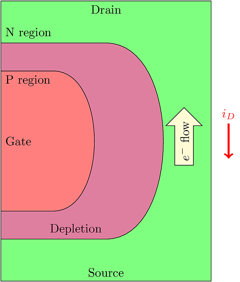
The JFET device can be classified both as a junction transistor and a field-effect transistor. The device consists of a doped semiconductor channel and an opposite-doped gate junction. The gate junction forms a depletion region within the channel. When the gate junction is reverse-biased, the depletion region grows into the channel, thereby reducing the effective channel width. The channel current is said to be “pinched” by the depletion layer. By increasing the reverse bias on the gate junction, the depletion region is widened, and the current decreases. Once the channel is fully depleted (i.e. when the depletion region extends across the entire depth of the channel) the current goes to zero.

Since the gate junction in a JFET is always reverse-biased, there is nearly zero gate current. This makes them very good transconductance amplifiers, however they are not good switches. A JFET only switches off when the channel is fully pinched (i.e. depleted), which happens at a gate voltage \(V_P\). The pinch-off voltage \(V_P\) is not well controlled, making it impossible to guarantee a voltage that will reliably turn off the device.
To avoid forward biasing the junction, the gate must be reverse biased with respect to both the source and drain. In practice, JFETs are often used with these constraints:
N-channel JFET: \(v_{\text{DS}}>0\) and \(v_{\text{GS}}<0\)
P-channel JFET: \(v_{\text{DS}}< 0\) and \(v_{\text{GS}}> 0\)
The device model for a JFET is similar to a MOSFET. For an N-channel JFET, we may define the JFET overdrive voltage as
\[v_{\text{OV}}= v_{\text{GS}}- V_P,\]
where \(v_{\text{GS}}\) and \(V_P\) are both negative. Then, like the MOSFET, the JFET has a saturation mode when \(v_{\text{DS}}>v_{\text{OV}}\), and the saturation current is given by
\[i_D = I_{DSS}\left(1-\frac{v_{\text{GS}}}{V_P}\right)^2,\]
where \(I_{DSS}\) is the current that flows when \(v_{\text{GS}}=0\).
When \(v_{\text{DS}}< v_{\text{OV}}\), the device operates in its linear mode and behaves like an adjustable resistor. In this mode, the device current is given by
\[i_D = \frac{2I_{DSS}}{V_P^2}\left(v_{\text{OV}}- \frac{v_{\text{DS}}}{2}\right)v_{\text{DS}}.\]
The device equations bear a resemblance to MOSFETs. The equations above govern the N-channel JFET. The complementary P-channel JFET has the same qualitative behavior but with reversed polarity, similar to the relationship between NMOS and PMOS behaviors.